Semiconductor Ecosystem for India: Need for a Multi-pronged Strategy
MARCH 2021
Manoj Soman
Chip Designer, Technology Advisor and Teacher
Synopsis
The unique geo-political transitions in the world today and the apprehensions of a number of nations regarding over-dependence of imports from China has given India a new opportunity window for creating a healthy Electronics and Semiconductors Ecosystem.
Govt of India’s important initiative on the Product Linked Incentive (PLI) scheme for Electronics Manufacturing is a great start and will significantly accelerate manufacturing, Assembly Test Marking Packaging (ATMP) side of the electronics ecosystem. The PLI scheme is already attracting Global smartphone manufactures to India, can potentially catalyse other ecosystem activities including fabless design, if suitable policy and incentive structures are put in place. The PLI like scheme for wearable device manufacturing is also being contemplated by the Government of India (GoI). All these initiatives will accelerate the Make in India and Atmanirbhar Bharat (self- reliance) vision of the Government.
The domestic Fabless semiconductor design ecosystem, which requires significantly less capital expenditure, forms a very critical & high impact component of the electronics ecosystem, needs to be addressed urgently. The fabless design activity will help India move up in the value chain with much higher Return-On-Investment. The PLI schemes therefore, needs to be suitably amended to accelerate the fabless semiconductor design activity as well.
Data and Telecom, along with cutting-edge technologies such as Artificial Intelligence, Machine Learning and Bioinformatics, have emerged as the “new Oxygen” in the 21st century. This underscores the enormous significance of the semiconductor industry which is at the heart of virtually all smart devices and processes. Today, India imports 100% of the chips, memory and display components required by its semiconductor industry and this has serious implications for India’s economy and national security. In a written reply to the Rajya Sabha on September 17, 2020, Mr. Sanjay Dhotre, Minister of State for Electronics and IT, said India’s electronic component imports for 2019-20 stood at Rs. 1.15 lakh crore out of which 37% came from China.
The Total Available Market (TAM) of the global semiconductor ecosystem has been pegged at US $1.78 T by Prof. Arogyaswami Paulraj and of this, the semiconductor and system design space – predominantly a Fabless activity – contributes to $1T of the TAM.
India can embark on a multi-pronged strategy to achieve critical mass by first making the fabless design houses ecosystem strong by training manpower and through research in good universities and institutions, leveraging the entrepreneurial aspirations of start-ups, defining our own specifications for domestic consumption, promoting collaborative clusters for the targeted domains and the introduction of a host of semiconductor policies and incentives by the Central and State governments.
While Fabs require long-term lead times, a solid foundation for future fab activity can be laid by establishing mini-fabs (mid-term, 2-3 years) and higher-end fabs (long-term, 3-7 years) through joint ventures with fabs like TSMC and GF in Taiwan, with irresistible incentives. Close cooperation and collaboration with Taiwan– a leader in the semiconductor components space– should constitute an important part of this strategy.
Given that India with its billion-strong population is one of the leading consumers of mobile phones, the immediate focus can be on PLI (production-linked incentive) schemes for Original Design Manufacturers (ODMs), Original Equipment Manufacturers (OEMs) and others for the manufacture of mobile phones and components such as BTLE/GPS/NavIC, Li-Ion batteries, Power Management ICs (PMIC), Mobile sensor and associated electronics, Wireless connectivity, Audio subsystems and creative wearable devices.
A. Introduction
Building a healthy Electronics and Semiconductors Ecosystem is one of the topmost priorities for India, as it is the key enabler for practically every initiative of national importance. One part of this is semiconductor fab, which has been India’s dream for many years. But previous attempts have not been very successful over the decades, barring a few state- owned fab facilities. This was because the critical issue of fabs had never been comprehensively addressed in the context of the larger semiconductor ecosystem and its key component, fabless design ecosystem, which needed to be accelerated as the first crucial step.
Now, a new opportunity window has presented itself, as India is going through some unique geo- political transitions which include:
- World’s issues with China
- Perceived urgent need for geographical decentralization of foundries for de-risking
- Significant shift in India’s international image and position
- Various Digital India initiatives fuelling demand
- Modernization of various Indian sectors including agro-tech
- Leveraging strong embedded and application software capabilities
- Impact of 5G technology
- Prime Minister’s strong focus on Make in India and Atmanirbhar Bharat
- PLI-based scheme for the manufacture of Mobile phones and also SPECS & EMC2
India needs to take the fullest advantage of these unique geo-political transitions, including ‘the China situation’; de-risking manufacturing, and India’s proximity to Taiwan in the context of chip fabrication. And most importantly, the Government of India’s (GoI) strong digital initiative and policies like PLI for mobile manufacturing. The PLI scheme is already a huge success in terms of the applications received from Global as well as Domestic Mobile Phone manufacturing companies and electronic components manufacturers. Production amounting to Rs. 10.5 lakh crore and Exports of Rs. 6.5 lakh crore is expected over the next 5 years.
B. Semiconductor Ecosystem Components
The Global Semiconductor ecosystem’s Total Available Market (TAM) is $ 1.78T [ref. Prof A Paulraj’s lecture at IESA Vision Summit 2020] out of which $1T is in the semiconductor and system design space which is predominantly a Fabless activity and the manufacturing of semiconductors is outsourced to dedicated pure-play Fabs like TSMC, GF etc. Fabs contribute to $ 550B of the TAM
The following few paragraphs summarize various semiconductor eco-system components that are relevant and India’s status on the same. These components have to reach a critical mass, to first make the fabless design houses ecosystem strong, followed by an indigenous fab capability leading to the realization of the dream of participation in the global semiconductor ecosystem.
- Competent Workforce of Semiconductor Technologists and Engineers supported by good universities/institutions for both, training manpower and research:
- India is very well placed on this with the presence of top semiconductor chip companies design centres like TI, Broadcom, Intel, Qualcomm, etc. with highly trained engineers for more than two decades now. There is also the presence of semiconductor product companies such as
- There is increased entrepreneurial aspiration among some of these highly trained individuals and groups, which needs to be systematically
- Critical Mass of Fabless Semiconductor Companies who manufacture their chips through fab facilities across the world and also have expertise in commercial chip development activities:
- India has many start-up companies but the spread is too thin in many areas leaving critical gaps and poor
- Strong Domestic Demand for Semiconductor Chips for consumption and for solving specific problems:
- In spite of high consumption of semiconductor chips, we do not define our own specifications. We use whatever is available internationally. This should change.
- Predictable and Semiconductor sector-friendly Policies and incentives from the Govt and States:
- A lot needs to be done
- Expertise in Planning and Executing Complex Mega Projects and process plants and the management of an ecosystem for procurement of raw materials, chemicals, etc. as chip making is less about electronics and more about chemistry, raw materials, process mastery, heavy equipment and supply chain:
- India has both public as well as private companies with strong expertise in this area, albeit in the non-semiconductor space which can be leveraged for the semiconductor fab domain through Joint We need a specific entity to take a Leadership Role here.
- Actual Fab Plant and allied capabilities such as assembly, testing and IC packaging, etc:
- There are just a few government-funded fabs like SCL but they are not state-of-the-art. A few companies exist in the testing and packaging space. India needs to take steps to exploit and strengthen its new-found political proximity to Taiwan
C.Long Term View – What Can India Do To Create This Ecosystem?
- Building Critical Mass in Fabless design eco-system is the first crucial step towards participation in the larger semiconductor ecosystem. Clearly, specific technology domains need to be identified for Fabless design activities, rather than spreading too thin. This is in our national
1a.Examples of domains would include Smartphone and wearable devices related ICs, Cyber security systems, electronics in agrotech, electronics in payment systems, renewable energy electronics, etc.
1b.Create collaborative clusters so that all the relevant allied technologies also get naturally built around it. Identify and promote the formation of the right kind of companies working in synergy to create accelerated growth.
1c. Create active repository of key problems in electronics that our nation is facing, along with specifications. Encourage formation of new start-ups around these problems and also strengthen the cluster ecosystem.
1d. Specific aspects of defence electronics such as navigation and NavIC/GPS compliant navigation ICs. These can be used in mobile phones too.
- Start planning on indigenous Fabs – Fabs requires very long lead times. Therefore, while focusing on building a fabless design ecosystem, India must simultaneously start laying a foundation for future Fab activity that will pick up 2 to 7 years down the line. This would be in terms of planning, building relationships and allied capabilities and policy Fabs need to be looked at and addressed differently in two distinct categories, namely:
2a: Mini-fabs (Mid-term 2-3 years): 180nm – 65nm nodes
The existing fabs can be upgraded and replicated much quicker and with a much lower budget which is 1/10th to 1/20th of the cost of modern advanced fab which cost around $ 5B. Designs up to 65nm technology nodes can cover a wide range of design space. This will be a great start and will accelerate many start-ups while meeting the critical domestic demand for semiconductors.
2a1. Open up SCL and ISRO foundries and start running shuttle programs for start-ups for prototyping.
2a2. Create/upgrade multiple low-cost mini-foundries across the country and include universities/institutions in this endeavour.
2a 3. Make (2a1) and (2a2) above easily accessible to innovative start-ups for prototyping. These can be effectively used in IoT, sensors, smart agriculture technologies and renewal energy applications. India does not need the latest semiconductor technology node for everything.
2a 4. Strengthen capabilities in materials by roping in institutes like NCL and IISc.
2a 5. Declare a must-have-indigenous-fabs policy as a long-term goal (similar to the space program strategy).
2b: Higher-end fabs (Long- term 3-7 years)
2b 1. Here, India must leverage her heightened political proximity to Taiwan and forge joint ventures with fabs like TSMC and GF to setup centres in the country with irresistible incentives.
2b 2. The Capabilities (as in Section B point no.5 above) of some private sector companies such as RIL or Tata can also be leveraged for forging such joint ventures as in 2b1 above. The Government can play a role as a part equity holder, if necessary.
3. Top-Down approach: Create a nodal agency
This agency will oversee the overall semiconductor ecosystem development – identify weak areas and engage the right institutions, companies and departments to first build and strengthen a Fabless design ecosystem, followed by indigenous Fabs, beginning with mini-fabs.
D. Immediate Term View: Smart Phones and Sub-systems
The GoI’s new PLI scheme for the electronics manufacturing is driving the manufacturing side of smartphones in India. This smartphone opportunity must also be leveraged as a vehicle to propel overall semiconductor ecosystem in India through right incentive schemes.
A typical smartphone (Figure1) has a variety of complex subsystems with the Application Processor at the heart. Each subsystem has its own peculiarities and ecosystems. Based on where we are currently, the subsystems that can be immediately focused upon are marked in red in Figure 1.
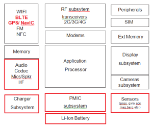
Figure 1: High level block diagram of a typical Smartphone
Other subsystems can be gradually added as we strengthen our capabilities on the fabless designs and the rest of the semiconductor ecosystem.
1. Li-Ion battery manufacturing for mobiles
- Leverage strong know-how available with ISRO for commercial use
- Custom battery making for lower costs
- We will have lateral benefits in other electronics needs like EV batteries
- Private players such as Sunwoda have set up manufacturing in India
2. Power Management ICs (PMIC) and Battery charger space
- This can be aligned with battery manufacturing
- A few start-ups have successfully developed PMICs
- These ICs can be both designed and fabricated in India
3. Mobile Sensor And Associated Electronics
- India has MEMS sensor fabrication Upgrade and leverage it for mobile sensors – like MEMS microphones and many other sensors
- Rope in ICs design houses: A few companies have developed the electronics for this
4. Wireless Connectivity
- Main wireless 4G data pump and baseband is a highly complex piece and should be dealt with later
- However, allied RF like Wifi/BTLE and particularly GPS can be focused upon
- We should leverage mandatory compliance to India’s NavIC specs
- Support commercialization of indigenous prototypes on NavIC For example, IITB Dhruva RFIC
5. Audio Subsystem
- India has expertise in audio Codec ICs and embedded SW for the same
6. Creative Wearable Devices tightly interfaced with smartphones
-
- There is a big opportunity for wearables in Many start-ups are active on the wearables.
- Focus on the ecosystem of fabless ICs and mechanical design for supporting the prototyping and commercialization,
- Develop creative apps using existing smartphone hardware/sensors for Indian Example: Farmer support systems dealing with soil/weather/crop data, market, pricing, real-time assistance. etc.
- GoI’s plan to offer the PLI like scheme for wearable devices manufacturing is very However, apart from the manufacturing, specific incentives should also be given for the design and fabrication of the sensors and the ICs required for wearable in India.
E. Accelerating The Fabless Design Ecosystem– Key Elements
We need to immediately address the following key elements on priority:
- Focus and attract the ODMs and OEMs in the mobile space leveraging PLI
- Mobile OEMs work with a variety of ODMs (Original Design Manufacturers) for their subsystems like app processor subsystem, radio and modems, sensors, battery, PMIC, display, peripherals, cameras, audio subsystems
- ODMs are in charge of their subsystems- specs, design and sourcing, and can potentially work with local IC suppliers for their design requirements
Hence the ODMs (as in the section-D above) should be given surgical focus and priority, as they are critical ecosystem components for India to enable and accelerate the growth of local Fabless Companies.
- The Government of India needs to target the selected subsystems and provide the right policies and irresistible incentives to those ODMs to set up their shops in India
- After this, rope in relevant fabless companies to support the ODMs in close proximity
- Initiate policy reforms in Govt grants scheme to enable grants directly to promising fabless start-ups/private sector
- Currently only institutions/universities get grants
- Constitute High Power Committees for each domain to select deserving private players/start- ups and support This will also ensure that the scheme is not misused
3. Create Accelerator Clusters
- For every cluster, establish an Experts Committee to Identify and nurture selected start-ups
- Provide initial funding and business-related mentoring (Approx. 1-2 Cr per design start-up)
- Make available Silicon Technology PDK and EDA tools for 18mo – 2yrs ( 5-10 Lac)
- Provide Test chip fabrication and prototyping financial support (Rs 30-40 Lac)
- SFAL (Semiconductor Fabless Accelerator Lab1)
- Israel Innovation Authority, IIA can be a good model to study closely2
4,Private players like RJIO need to setup Fabless semiconductor-specific ventures
-
- Align with new PLI policy for mobile manufacturing in India
5,Opening up local SCL/ISRO and Fabs, etc. for private players/start-ups
-
-
- 18um fab is a good start for many IC developments for Indian needs – Power Management I ICs, Battery electronics and IoT sensors
- Provide specific focus to the MEMS sensors for mobile electronics
- Make available Foundry PDKs to private players to design products
- Start regular shuttle program at SCL for prototyping test-chips
-
6.Initiate a parallel thread to attract mini-fabs and Joint Venture fabs with big players like TSMC and GF
F. Overall Approach
- Undertake efforts to accelerate and grow fabless design activity and ecosystem to a critical mass and enable fabless start-ups
- Attract ODMs to set-up shops and set-up fabless design activity clusters
- Fabs need a long lead time and hence the Government should start planning for them in It may be emphasised that bringing up mini-fabs will be crucial for India 3-5 years down the line
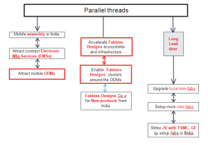
Figure 2: Steps to accelerate fabless design activity and fab setup in India
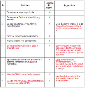
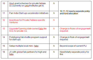
G. Semiconductor Ecosystem Needs And Status On Existing PLI Scheme Support
The semiconductor ecosystem needs to be looked and addressed from the tops-down. Following table summarizes the semiconductor activities, where the existing PLI scheme support is available and set of suggestions to support the unaddressed components of the ecosystem. We need multiple schemes like the PLI for manufacturing, to tackle this comprehensively.
Annexure
Manoj Soman is an Analog, RF, Mixed-signal IC, and DSP architect and designer with more than 28 years of hands-on experience in Radio Frequency transceivers, audio/ video/ communication ICs, customizable DSPs, SerDes, etc and has led numerous full-chip IC design projects. He worked with Texas Instruments, CirrusLogic, Alereon, Mindtree, Cadence and was VP of R&D of a high- speed SerDes startup which got acquired by Synopsys Inc. His area of interest is pushing the designs for area, power, and speeds through architectural and circuit innovations. He is also passionate about teaching. Manoj is a Gold medallist in B.E.(Hons)- Electronics Engineering from Bombay University and Masters in Electrical Communication Engineering from Indian Institute of Science, Bangalore. He holds 11 US Patents.
Dr. Prakash Hebalkar pioneered the Indian software export industry through Tata Burroughs Ltd and signed the nation’s first MOU for a fabless design centre with VLSI Technologies. Skilled in Business Strategy, Business Planning, IT Strategy and Management, and Mergers and Acquisitions, he is a strong entrepreneurship oriented professional with a Doctor of Science (D.Sc.) focused in Computer Science and Economics from M.I.T.
Vikas Deshmukh is former Managing Director, Tata Elxsi and former Chairperson, Confederation of Indian Industry, Karnataka. Over the last decade he has mentored a number of start-up companies in the USA and India.
Commodore Anand Khandekar (Retd); Served the Indian Navy for 25 years where he worked for five frontline ships including Aircraft Carrier Vikrant and was Training Commander of Indian Navy’s premier Weapons and Electronics Training Establishment at Jamnagar. Also served as the Director of Weapons and Electronics at the Naval HQ in New Delhi. Ex-Chief Mentor and Director, Nvidia Graphics.
Sanjay Kanvinde has 23 years experience in the Energy Industry. Over different assignments, he has worked in the functional areas of Research & Development, Knowledge Management, Business Development and Corporate IT Management. He is the co-founder of Lavni Ventures.
References
1https://sfalcoe.org/ 2https://innovationisrael.org.il/en/ Technical information available on the internet on smartphones, semiconductors, sensors etc
Indian Electronics Industry – Interdependence or Self Reliance” , IESA vision summit 2020 lecture by Arogyaswami Paulraj